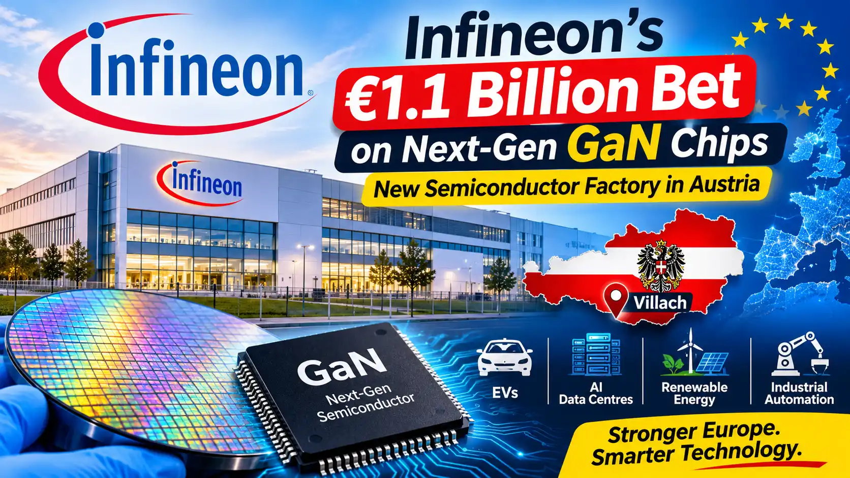
Germany-based semiconductor manufacturer Infineon Technologies is taking a major step towards strengthening Europe’s semiconductor industry with an investment of approximately €1.1 billion in a new 300-mm Gallium Nitride (GaN) Power Semiconductor Manufacturing Facility in Villach, Austria.
The new facility will manufacture next-generation GaN-based power semiconductor chips. These chips can be used in several industries, including Electric Vehicles (EVs), Renewable Energy, AI Data Centres, Industrial Equipment, Fast Chargers and other electronic devices.
The primary objective of this investment is to meet growing global demand for energy-efficient power semiconductors, expand Europe’s semiconductor manufacturing capabilities and strengthen Infineon’s position in the Power Electronics industry.
According to the company’s plan, production at the facility is expected to begin by the end of 2027.
This investment is particularly important because the rapid expansion of AI Data Centres, Electric Vehicles and Renewable Energy projects is increasing demand for semiconductor technologies that can manage and convert electricity more efficiently.
Key Highlights
| Particulars | Details |
| Company | Infineon Technologies AG |
| Company Country | Germany |
| Investment | €1.1 Billion |
| Investment Country | Austria |
| Manufacturing Location | Villach |
| Technology | Gallium Nitride (GaN) |
| Wafer Size | 300 mm |
| Government Aid | Up to €319 Million |
| Production Start | End of 2027 (planned) |
| Investment Period | Until 2034 |
| Target Industries | AI, EV, Energy, Robotics |
| Market Forecast | $3.5 Billion by 2031 |
What Is Infineon Technologies?
Infineon Technologies AG is a leading semiconductor manufacturing company. The company develops semiconductor chips and electronic solutions used for power management, automotive systems, industrial applications and electronic devices.
Infineon’s technologies are widely used in Electric Vehicles, Solar Inverters, Wind Energy Systems, Data Centres, Smartphones, Industrial Machines and Smart Devices.
The company’s major business segments include:
- Automotive: Semiconductor chips for Electric Vehicles, Vehicle Control Systems, Battery Management and Automotive Electronics.
- Green Industrial Power: Power semiconductors for industrial machines, renewable energy systems and electricity management.
- Power & Sensor Systems: Semiconductor solutions for smartphones, computers, consumer electronics and power management.
- Connected Secure Systems: Security chips, microcontrollers and semiconductor solutions for IoT devices.
Company Overview
| Particulars | Details |
| Company | Infineon Technologies AG |
| Headquarters | Neubiberg, Germany |
| Established | 1999 |
| Industry | Semiconductor |
| Stock Exchange | Frankfurt Stock Exchange |
| Stock Ticker | IFX |
| FY2025 Revenue | Approximately €14.7 Billion |
| Employees | Approximately 57,000 |
| Major Investment Location | Villach, Austria |
Why Is Infineon Investing €1.1 Billion?
Global electricity consumption is increasing rapidly, driven by several industries and technologies.
Some of the major factors include:
- The expansion of AI and Cloud Computing Data Centres.
- Increasing adoption of Electric Vehicles.
- Growth in Solar and Wind Energy Projects.
- Expansion of Industrial Automation and Robotics.
- Rising demand for Fast Charging and Power Electronics.
However, generating electricity is not enough. It must also be converted, controlled and delivered to electronic devices at the required voltage and power levels with minimum energy loss.
For example, a large AI Data Centre contains thousands of high-performance servers that require a continuous and reliable electricity supply. Electricity must pass through multiple conversion stages before reaching the processors and other components.
If significant energy is lost as heat during this process, electricity costs and cooling requirements increase.
Infineon aims to address these challenges by expanding its manufacturing capacity for next-generation GaN Power Semiconductors.
What Is Gallium Nitride (GaN) Semiconductor Technology?
Gallium Nitride, commonly known as GaN, is a special semiconductor material used to manufacture electronic components that control and convert electricity.
Silicon-based semiconductors are widely used in today’s electronic devices. However, GaN can offer better performance in certain high-power and high-frequency applications.
Major Advantages of GaN Technology
- Helps reduce energy losses during power conversion.
- Supports faster electrical switching.
- Can reduce heat generation in suitable applications.
- Enables smaller power electronic devices.
- Helps develop systems with higher power density.
Simple Example
Consider two fast chargers. An older charger design may lose more energy as heat while converting electricity. A well-designed GaN-based charger can perform the same power conversion with lower energy losses.
This creates opportunities to develop smaller and more efficient chargers.
However, GaN is not automatically better than silicon in every application. Both materials have different advantages, and the choice depends on factors such as voltage, power requirements, cost and application.
What Is 300-Millimeter Wafer Technology?
One of the most important features of Infineon’s investment is its plan to manufacture GaN Power Semiconductor Chips using 300-millimeter wafers.
A wafer is a thin, circular semiconductor material on which multiple small electronic chips are manufactured simultaneously. These chips are later separated and packaged for use in electronic devices.
Traditionally, 200-mm wafers have been used in GaN Power Semiconductor manufacturing. Infineon is now moving towards the larger 300-mm wafer format.
Comparison Between 200-mm and 300-mm Wafers
| Particulars | 200-mm Wafer | 300-mm Wafer |
| Diameter | 200 mm | 300 mm |
| Surface Area | Approx 31,416 mm² | Approx 70,686 mm² |
| Chip Production | Comparatively lower | Approx 2.3 times higher |
| Manufacturing Efficiency | Lower | Potentially higher |
According to Infineon, a 300-mm wafer can accommodate approximately 2.3 times more chips than a 200-mm wafer.
This means that manufacturers can potentially produce more semiconductor chips while processing a similar number of wafers.
It can also help reduce manufacturing costs per chip and support large-scale production.
However, this does not mean that total production costs will automatically decrease by the same proportion. Actual costs depend on manufacturing equipment, production yield, processing requirements and other expenses.
Infineon’s important achievement is its effort to move 300-mm GaN technology from research and development towards commercial high-volume manufacturing.
Where Will the New Manufacturing Facility Be Located?
The new manufacturing facility will be developed in Villach, Austria, located in the southern part of the country.
Infineon already operates a major semiconductor manufacturing facility in Villach. Instead of building an entirely new factory on a separate site, the company plans to utilise and upgrade its existing cleanroom infrastructure.
A cleanroom is a specially controlled manufacturing environment where dust and tiny airborne particles are carefully restricted. Semiconductor production requires extremely clean conditions because even microscopic particles can damage sensitive components.
The project will involve:
- Expanding and modernising existing cleanroom infrastructure.
- Developing new manufacturing capabilities for 300-mm GaN wafers.
- Strengthening the connection between power semiconductor research and manufacturing.
- Further developing Villach as a global competence centre for power semiconductors.
Infineon has approximately 5,800 employees in Austria, including around 4,800 employees at its Villach site.
Details of the €1.1 Billion Investment
Infineon plans to invest approximately €1.1 billion in the project.
The investment will be deployed in phases to upgrade existing manufacturing infrastructure and develop additional production capabilities.
| Particulars | Details |
| Investing Company | Infineon Technologies |
| Total Investment | Approximately €1.1 Billion |
| Investment Location | Villach, Austria |
| Technology | Gallium Nitride (GaN) |
| Wafer Size | 300 mm |
| Project | High-Volume GaN Manufacturing |
| Investment Timeline | Until 2034 |
| Production Start | Planned by the end of 2027 |
| Government Support | Up to €319 Million |
| Main Objective | Expand Power Semiconductor Manufacturing |
An important point is that the €1.1 billion represents the total project investment. The government support of up to €319 million is included within the project’s overall financing framework. It should not be added again to the investment amount to calculate a total of €1.419 billion.
The government support is being provided by Austria through State Aid, which received European Commission approval on 27 October 2026. The formal funding commitment is subject to the applicable procedures.
€319 Million Government Support Under the European Chips Act
European governments are also playing an important role in this project.
The European Commission has approved up to €319 million in Austrian State Aid for Infineon’s investment.
This support is aligned with the objectives of the European Chips Act, an important European Union initiative designed to strengthen semiconductor manufacturing, research and technology development across Europe.
The main reason behind this initiative is that countries and regions such as Taiwan, South Korea, China, Japan and the United States play major roles in the global semiconductor manufacturing industry.
Europe wants to expand its domestic chip manufacturing capabilities and reduce dependence on foreign suppliers.
Under the approved support framework, Infineon will also contribute to the development of the wider European semiconductor ecosystem.
This includes:
- Collaboration with startups and small businesses.
- Supporting universities and research institutions.
- Providing semiconductor technology-related training.
- Developing new semiconductor engineers and skilled workers.
- Strengthening cooperation between research and manufacturing.
Therefore, government support is not limited to establishing a manufacturing facility for one company. It is also intended to strengthen Europe’s wider semiconductor industry.
Applications of GaN Chips Across Different Industries
The new GaN manufacturing facility could serve several rapidly growing industries.
1. AI Data Centres
AI Data Centres contain large numbers of GPUs, servers and networking equipment. All these systems require a continuous and stable electricity supply.
GaN-based power semiconductors can help convert and control electricity more efficiently. This creates opportunities to reduce energy losses and heat generation.
For example, large AI training facilities consume significant amounts of electricity. Even a small improvement in power conversion efficiency can potentially save considerable amounts of energy.
2. Electric Vehicles (EVs)
Electric Vehicles use power electronics to manage electricity flowing from the battery to the motor.
GaN technology can be used in applications such as EV charging systems, onboard chargers and selected power conversion systems.
It can help manufacturers develop smaller and more efficient power electronic components.
3. Renewable Energy
Solar panels and wind turbines require power conversion systems to make generated electricity suitable for batteries and electricity grids.
GaN-based semiconductors can contribute to improving the efficiency of these systems.
4. Robotics and Industrial Automation
Modern factories increasingly use robots, automated machines and industrial motors.
These machines require semiconductor components to control electricity and power delivery. GaN technology can help develop compact and efficient power systems for industrial applications.
5. Consumer Electronics and Fast Chargers
GaN technology is already being used in compact fast chargers, laptop adapters and other electronic power supplies.
It enables manufacturers to develop chargers that can deliver higher power from relatively small devices.
How Large Could the GaN Semiconductor Market Become?
One of the major reasons behind Infineon’s investment is the growth potential of GaN technology.
According to the Power GaN 2026 Report by Yole Group, cited by Infineon, the global GaN Power Semiconductor market could reach approximately $3.5 billion by 2031.
The market is projected to grow at an estimated compound annual growth rate (CAGR) of approximately 35% between 2025 and 2031.
GaN Power Semiconductor Market – Forecast
$3.5 Billion: Projected global market size by 2031
Expected CAGR: ~35%
2025–2031 | Industry forecast cited by Infineon
This forecast indicates that GaN technology could become one of the faster-growing segments of the semiconductor industry.
However, this represents an estimated market size, not a forecast of Infineon’s individual revenue or profit.
How Will This Investment Benefit Europe?
The project could benefit not only Infineon but also the wider European semiconductor ecosystem.
1. Greater Semiconductor Manufacturing Independence
Europe will be able to increase the domestic production of important semiconductor components. This could help reduce dependence on overseas manufacturing.
2. Development of New Technologies
300-mm GaN manufacturing could strengthen Europe’s position in the development and production of next-generation power semiconductors.
3. Employment Opportunities
The expansion could create demand for skilled engineers, semiconductor technicians, research scientists and other technical professionals.
However, the company has not yet announced a confirmed number of additional jobs specifically associated with this project.
4. Benefits for Local Industries
Semiconductor manufacturing requires equipment suppliers, industrial service providers, research organisations and universities. The project could create additional business opportunities for these organisations.
5. Support for AI and EV Industries
The project could help provide more efficient power semiconductors for the expansion of AI Data Centres, Electric Vehicles and Renewable Energy projects across Europe.
What Challenges Could Infineon Face?
Although the project offers significant opportunities, there are several challenges that Infineon will need to address.
- High Manufacturing Costs: Scaling 300-mm GaN manufacturing successfully requires significant investment and technical expertise.
- Production Yield: The company must ensure that a high percentage of chips produced from each wafer meet quality standards.
- Market Competition: Semiconductor companies in the United States, China and other countries are also developing GaN technologies.
- Customer Demand: The new manufacturing capacity will need sufficient demand from AI, EV and industrial customers.
- Project Execution: Infineon must complete its manufacturing expansion according to its planned investment timeline through 2034.
The company’s ability to begin production by the end of 2027 and gradually scale commercial manufacturing will be an important factor in determining the project’s success.
What Does This Project Mean for the Future of Infineon?
Infineon’s investment indicates an important shift in the semiconductor industry.
Semiconductor manufacturers are no longer focusing only on developing smaller and faster processors. They are also investing heavily in chips that can manage and utilise electricity more efficiently.
As AI Data Centres, Electric Vehicles, Renewable Energy and Robotics continue to expand, Power Electronics will become increasingly important.
The transition to high-volume manufacturing using 300-mm GaN wafers could give Infineon an opportunity to increase production capacity and improve manufacturing economics.
If the project succeeds, Villach could become one of the world’s important manufacturing centres for GaN Power Semiconductors.
Sources: Infineon Technologies – Official Announcement | European Commission – State Aid Approval | Yole Group – Power GaN 2026 Report