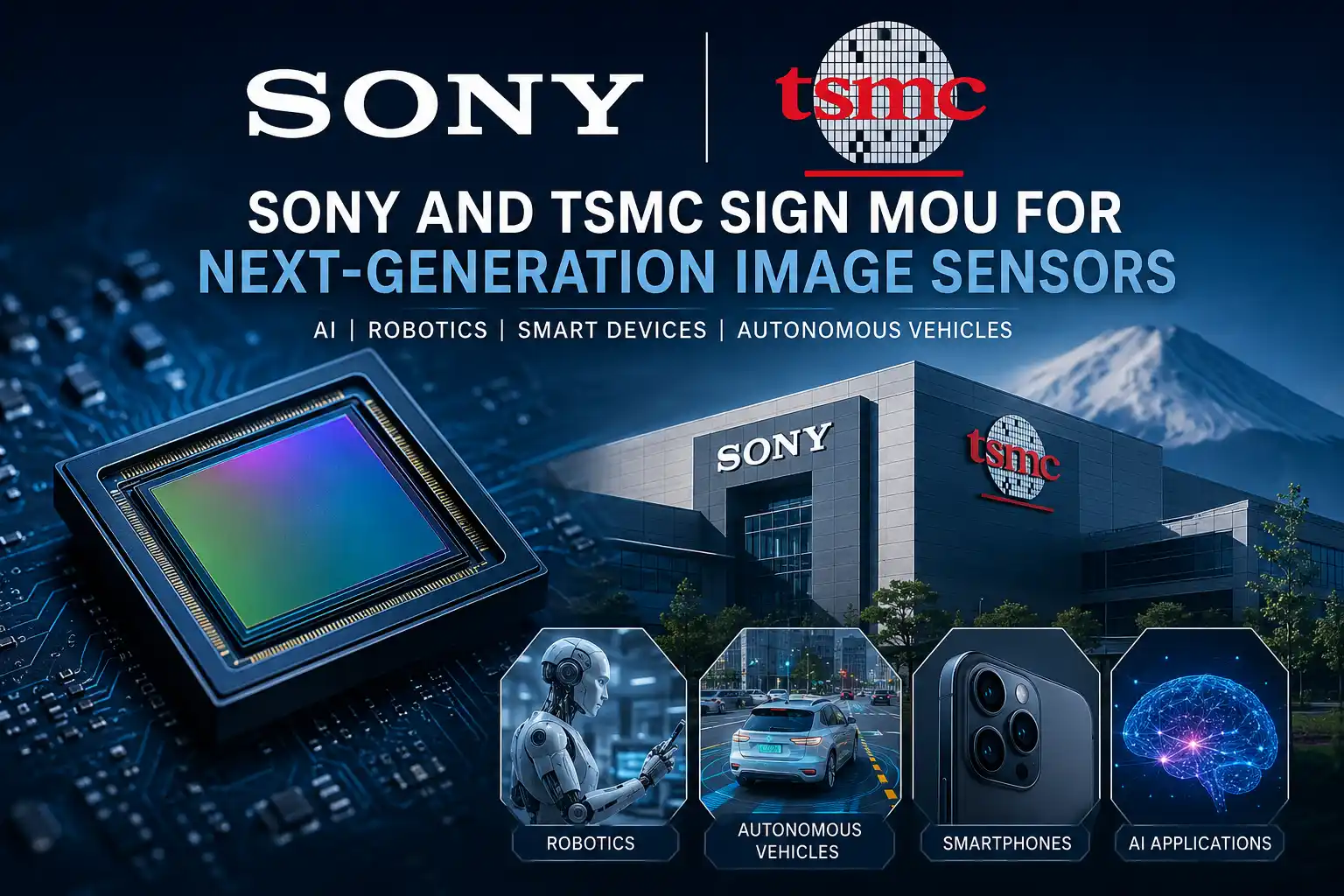
In a major development for the global semiconductor industry, Sony Semiconductor Solutions and Taiwan-based chip manufacturing leader TSMC have signed a Memorandum of Understanding (MoU) to jointly develop and manufacture next-generation image sensors in Japan. The partnership is expected to play an important role in the future of artificial intelligence (AI), robotics, autonomous vehicles, smartphones, and industrial automation.
The announcement has attracted significant attention across the technology industry because image sensors are becoming one of the most important components in modern AI-powered devices. With demand for advanced sensing technology growing rapidly worldwide, the collaboration between Sony and TSMC is being viewed as a strategic move to strengthen their positions in the global semiconductor market.
Sony and TSMC Plan New Joint Venture in Japan
According to the announcement, the two companies are planning to establish a new joint venture (JV) in Koshi City, Kumamoto Prefecture, Japan. Sony will hold the majority stake and maintain operational control of the venture. The facility is expected to be integrated with Sony’s new semiconductor fabrication infrastructure in the region.
The collaboration will combine:
- Sony’s global leadership in CMOS image sensor design
- TSMC’s advanced semiconductor manufacturing technologies and process expertise
The companies aim to create next-generation image sensors designed for future AI-driven applications that require faster processing, improved image quality, low power consumption, and enhanced sensing capabilities.
Industry analysts believe this partnership could significantly strengthen Japan’s semiconductor ecosystem at a time when countries worldwide are focusing on chip supply chain security and advanced technology manufacturing.
Why Image Sensors Are Becoming More Important
Image sensors are semiconductor devices that capture light and convert it into digital signals. These sensors are the core technology behind:
- Smartphone cameras
- DSLR and mirrorless cameras
- CCTV and surveillance systems
- Autonomous driving systems
- Medical imaging equipment
- Industrial robots
- AI-powered smart devices
As AI systems become more advanced, devices increasingly rely on high-quality visual data to make decisions. This has made image sensors one of the fastest-growing segments within the semiconductor industry.
Sony is already the world leader in CMOS image sensors, supplying components to several global smartphone manufacturers. Its sensors are widely used in premium smartphones because of their strong performance in low-light photography, autofocus, and AI image processing.
Meanwhile, TSMC is the world’s largest semiconductor foundry company and manufactures advanced chips for major technology companies such as Apple, Nvidia, AMD, Qualcomm, and many others. The partnership allows Sony to benefit from TSMC’s cutting-edge chip manufacturing technologies while helping TSMC expand deeper into the advanced sensor market.
Focus on AI and “Physical AI” Applications
One of the key highlights of the partnership is the companies’ focus on “Physical AI.” This term refers to AI systems capable of interacting with and understanding the physical world through sensors and real-time data processing.
The new image sensors are expected to support applications such as:
- Autonomous vehicles
- Robotics and humanoid robots
- Smart factories
- Industrial automation systems
- AI-powered security and surveillance
- Smart healthcare devices
- Edge AI computing
Future AI systems require not only advanced processors but also highly accurate sensing technologies that can detect motion, depth, lighting, objects, and environmental changes in real time. This is where next-generation image sensors become extremely important.
Experts believe that demand for these sensors could increase sharply over the next decade as AI-powered devices become more common in daily life and industrial operations.
Semiconductor Competition Is Increasing Worldwide
The Sony-TSMC partnership also comes at a time when the global semiconductor industry is witnessing intense competition and geopolitical pressure.
Countries including the United States, Japan, China, South Korea, and members of the European Union are investing heavily in semiconductor manufacturing to reduce dependence on foreign supply chains.
Japan has been actively trying to rebuild its semiconductor manufacturing strength through partnerships with global companies like TSMC. The Japanese government has already provided support for semiconductor investments in Kumamoto, where TSMC’s JASM project is under development.
The new image sensor partnership could further strengthen Japan’s position in advanced semiconductor technologies.
Existing Collaboration Between Sony and TSMC
Sony and TSMC are not new partners. The two companies are already working together through Japan Advanced Semiconductor Manufacturing (JASM), a semiconductor manufacturing project located in Kumamoto. The project focuses on producing advanced chips for automotive, industrial, and consumer electronics applications.
The latest MoU is expected to expand the relationship further by focusing specifically on image sensor technology, which is considered one of the most strategically important semiconductor sectors for the future AI economy.
Investment Discussions and Expansion Plans
The companies clarified that the agreement is currently non-binding and discussions regarding final investment amounts, ownership structure, and operational details are still ongoing.
Reports suggest that the expansion could happen in multiple phases depending on:
- Global demand for image sensors
- AI market growth
- Automotive industry requirements
- Semiconductor market conditions
Analysts believe the project may involve billions of dollars in long-term investment if production scales successfully.
Impact on Smartphones and Consumer Electronics
The partnership could bring major improvements to future smartphone cameras and consumer electronics devices.
Potential benefits may include:
- Better low-light photography
- Faster autofocus systems
- Improved AI image processing
- Higher dynamic range
- More energy-efficient camera systems
- Enhanced augmented reality (AR) and mixed reality experiences
As smartphone brands increasingly compete on camera performance, advanced image sensor technology has become a major differentiator in the premium device market.
Benefits for the Automotive Industry
The automotive sector is also expected to benefit significantly from the partnership.
Modern autonomous and assisted-driving systems require multiple high-performance cameras and sensors to:
- Detect obstacles
- Recognize traffic signs
- Monitor lanes
- Improve safety systems
- Enable autonomous navigation
Next-generation image sensors with better accuracy and real-time processing capabilities could improve the reliability and safety of future autonomous vehicles.
What Company Executives Said
Sony Semiconductor Solutions CEO Shinji Sashida stated that the partnership would combine the strengths of both companies to accelerate innovation in image sensor technology and support future AI applications.
TSMC Senior Vice President Kevin Zhang described the collaboration as an important milestone for advancing sensing technologies in the AI era and strengthening semiconductor manufacturing capabilities in Japan.
Market Reaction and Industry Outlook
Industry experts believe the collaboration reflects the growing importance of specialized semiconductor technologies beyond traditional processors and memory chips.
As AI systems evolve, advanced sensors are expected to become a critical part of future computing infrastructure. Companies that control sensor technology may gain a major competitive advantage in the next generation of AI hardware.
The Sony-TSMC partnership could therefore become one of the most important collaborations in the global image sensor industry over the coming years.
Outcome
Sony and TSMC’s new strategic MoU for next-generation image sensors marks a major development in the semiconductor and AI industries. By combining Sony’s expertise in image sensor technology with TSMC’s world-leading semiconductor manufacturing capabilities, the partnership aims to develop advanced sensing technologies for future AI-powered applications.
The collaboration is expected to benefit industries ranging from smartphones and robotics to autonomous vehicles and industrial automation. If successfully implemented, the project could strengthen Japan’s semiconductor ecosystem while also helping Sony and TSMC expand their influence in the rapidly growing global AI and semiconductor markets.
Source: sony press


